Avalanche Photodiode Manufacturing in 2025: Navigating Explosive Growth, Next-Gen Technologies, and Global Market Shifts. Discover How Industry Leaders Are Shaping the Future of High-Sensitivity Photodetection.
- Executive Summary: Key Trends and 2025 Outlook
- Market Size, Growth Rate, and Forecasts to 2030
- Technological Innovations in Avalanche Photodiodes
- Key Applications: Telecom, LIDAR, Medical, and Beyond
- Competitive Landscape: Leading Manufacturers and New Entrants
- Supply Chain Dynamics and Regional Production Hubs
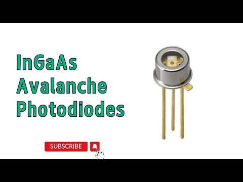
- Materials Science: Advances in Silicon, InGaAs, and Emerging Compounds
- Regulatory Standards and Industry Certifications
- Strategic Partnerships, M&A, and Investment Trends
- Future Outlook: Opportunities, Challenges, and Disruptive Forces
- Sources & References
Executive Summary: Key Trends and 2025 Outlook
Avalanche photodiode (APD) manufacturing is entering a pivotal phase in 2025, driven by surging demand from optical communication, LiDAR, medical imaging, and quantum technology sectors. The global push for higher-speed data transmission and advanced sensing capabilities is accelerating innovation in APD design, materials, and fabrication processes. Key trends shaping the industry include the transition to silicon and InGaAs-based APDs, miniaturization for integration into photonic circuits, and the adoption of automated, high-yield manufacturing lines.
Leading manufacturers such as Hamamatsu Photonics, Excelitas Technologies, and First Sensor AG (now part of TE Connectivity) are expanding their production capacities and refining wafer-level packaging techniques to meet the growing requirements of telecom and automotive customers. Hamamatsu Photonics continues to invest in advanced APD fabrication, focusing on low-noise, high-gain devices for 5G/6G infrastructure and next-generation LiDAR. Excelitas Technologies is leveraging its expertise in both discrete and array APDs, targeting medical imaging and industrial automation markets.
Material innovation remains a core focus, with manufacturers optimizing silicon APDs for visible and near-infrared applications, while indium gallium arsenide (InGaAs) APDs are being tailored for longer-wavelength detection, crucial for fiber-optic communications and quantum cryptography. The integration of APDs into silicon photonics platforms is gaining momentum, enabling compact, high-performance receiver modules for data centers and automotive sensors. Companies are also exploring hybrid integration and monolithic approaches to further reduce size and cost while improving reliability.
Automation and quality control are being enhanced through the adoption of AI-driven inspection systems and advanced process monitoring, aiming to boost yields and ensure device uniformity. Environmental and regulatory considerations are prompting investments in greener manufacturing processes and compliance with international standards, particularly as APDs find increasing use in safety-critical applications.
Looking ahead, the APD manufacturing sector is expected to see continued capacity expansion and technology upgrades through 2025 and beyond. Strategic partnerships between device makers, foundries, and system integrators are likely to accelerate the commercialization of next-generation APDs. As demand from quantum communication, automotive LiDAR, and high-speed optical networks intensifies, manufacturers with robust R&D pipelines and scalable production capabilities—such as Hamamatsu Photonics, Excelitas Technologies, and First Sensor AG—are well positioned to lead the market.
Market Size, Growth Rate, and Forecasts to 2030
The global avalanche photodiode (APD) manufacturing sector is positioned for robust growth through 2030, driven by expanding applications in optical communication, LiDAR, medical imaging, and industrial sensing. As of 2025, the market is characterized by increasing demand for high-speed, high-sensitivity photodetectors, particularly in the telecommunications and automotive sectors. The proliferation of 5G networks and the rapid development of autonomous vehicles are key factors accelerating APD adoption.
Major manufacturers such as Hamamatsu Photonics, Excelitas Technologies, and First Sensor AG (a part of TE Connectivity) are expanding their production capacities and investing in advanced fabrication technologies to meet rising global demand. Hamamatsu Photonics, for example, continues to lead in the development of silicon and InGaAs APDs, targeting both telecom and scientific instrumentation markets. Excelitas Technologies is focusing on high-reliability APDs for aerospace and defense, while First Sensor AG leverages its expertise in custom sensor solutions for industrial and medical applications.
In terms of market size, industry estimates for 2025 place the global APD market value in the range of several hundred million USD, with a compound annual growth rate (CAGR) projected between 7% and 10% through 2030. This growth is underpinned by the increasing integration of APDs in fiber-optic communication systems, where their ability to amplify weak optical signals is critical for long-distance, high-bandwidth data transmission. The automotive sector, particularly in LiDAR-based advanced driver-assistance systems (ADAS), is expected to be a significant growth driver, as manufacturers seek photodetectors with fast response times and high gain.
Geographically, Asia-Pacific remains the largest and fastest-growing region for APD manufacturing, led by investments in telecommunications infrastructure and automotive innovation. Companies such as Hamamatsu Photonics (Japan) and Kyosemi Corporation (Japan) are prominent players in this region, while European and North American firms continue to focus on high-value, specialized applications.
Looking ahead to 2030, the APD manufacturing sector is expected to benefit from ongoing advances in semiconductor materials, such as the adoption of InGaAs and other III-V compounds, which enable higher sensitivity and broader spectral response. Strategic partnerships between device manufacturers and system integrators are likely to accelerate innovation and market penetration. Overall, the outlook for avalanche photodiode manufacturing is strongly positive, with sustained growth anticipated across multiple high-tech industries.
Technological Innovations in Avalanche Photodiodes
Avalanche photodiode (APD) manufacturing is undergoing significant technological innovation as the demand for high-speed, high-sensitivity photodetectors grows across sectors such as optical communications, LiDAR, medical imaging, and quantum technologies. In 2025, manufacturers are focusing on improving device performance, yield, and integration capabilities, while also addressing cost and scalability challenges.
A key trend is the transition from traditional silicon-based APDs to compound semiconductor materials such as indium gallium arsenide (InGaAs) and silicon carbide (SiC). These materials offer superior sensitivity in the near-infrared and extended wavelength ranges, which is critical for applications like fiber-optic communication and advanced sensing. Leading manufacturers such as Hamamatsu Photonics and Excelitas Technologies are investing in proprietary epitaxial growth techniques and wafer processing to enhance the uniformity and reliability of their APD products.
Another innovation is the integration of APDs with complementary metal-oxide-semiconductor (CMOS) technology. This enables the fabrication of APD arrays and single-photon avalanche diodes (SPADs) directly on CMOS chips, facilitating compact, low-power, and scalable solutions for imaging and time-of-flight applications. Companies like ON Semiconductor are advancing CMOS-compatible APD manufacturing, enabling mass production for automotive LiDAR and 3D sensing markets.
Automated wafer-level testing and packaging are also being adopted to improve throughput and reduce costs. Manufacturers are implementing advanced photolithography, plasma etching, and passivation techniques to achieve tighter control over device parameters such as breakdown voltage and gain uniformity. First Sensor, a subsidiary of TE Connectivity, is notable for its focus on high-volume, high-reliability APD production, leveraging automated assembly lines and in-house testing capabilities.
Looking ahead, the outlook for APD manufacturing is shaped by the push towards higher pixel densities, lower noise, and greater integration with photonic and electronic circuits. The emergence of silicon photonics platforms and hybrid integration methods is expected to further drive innovation, enabling new device architectures and applications. As the industry moves into the latter half of the decade, collaborations between device manufacturers, foundries, and system integrators will be crucial for scaling up production and meeting the evolving requirements of next-generation photonic systems.
Key Applications: Telecom, LIDAR, Medical, and Beyond
Avalanche photodiodes (APDs) are critical components in a range of high-sensitivity photodetection applications, with manufacturing trends in 2025 reflecting both technological advances and expanding end-use markets. The telecom sector remains a primary driver, as APDs are integral to optical receivers in fiber-optic communication systems, where their internal gain enables detection of weak signals over long distances. Leading manufacturers such as Hamamatsu Photonics and First Sensor AG (now part of TE Connectivity) continue to supply APDs tailored for high-speed, low-noise performance, supporting the ongoing rollout of 5G and the anticipated growth of 6G infrastructure.
In LIDAR (Light Detection and Ranging), APDs are favored for their fast response and high sensitivity, essential for automotive applications such as advanced driver-assistance systems (ADAS) and autonomous vehicles. Companies like Hamamatsu Photonics and onsemi are actively developing APD arrays and modules optimized for LIDAR, focusing on improved uniformity, reduced crosstalk, and higher quantum efficiency. The automotive sector’s push for higher-resolution, longer-range LIDAR is expected to drive further innovation in APD manufacturing processes, including wafer-level packaging and integration with CMOS electronics.
Medical imaging is another significant application area, particularly in positron emission tomography (PET) and computed tomography (CT) scanners. APDs offer advantages over traditional photomultiplier tubes, such as compactness, immunity to magnetic fields, and lower operating voltages. Hamamatsu Photonics and Excelitas Technologies are among the suppliers providing APDs and silicon photomultiplier (SiPM) arrays for medical device manufacturers, with ongoing improvements in noise reduction and photon detection efficiency.
Beyond these established sectors, APDs are increasingly used in scientific instrumentation, quantum communication, and industrial sensing. The trend toward miniaturization and integration is prompting manufacturers to invest in advanced semiconductor processing, such as silicon and InGaAs APDs, to address the needs of emerging applications. Hamamatsu Photonics and onsemi are notable for their broad APD portfolios, while Excelitas Technologies is recognized for custom solutions and module integration.
Looking ahead, the outlook for APD manufacturing in 2025 and the following years is shaped by the convergence of high-speed communications, autonomous mobility, and precision medical diagnostics. Manufacturers are expected to focus on yield improvement, cost reduction, and the development of application-specific APD designs, leveraging advances in materials and device architecture to meet the evolving demands of these key markets.
Competitive Landscape: Leading Manufacturers and New Entrants
The competitive landscape of avalanche photodiode (APD) manufacturing in 2025 is characterized by a mix of established global players and a growing cohort of innovative new entrants. The sector is driven by surging demand from applications in optical communication, LiDAR, medical imaging, and quantum technologies. Leading manufacturers continue to invest in advanced fabrication processes, while new entrants are leveraging niche technologies and regional opportunities to gain market share.
Among the established leaders, Hamamatsu Photonics remains a dominant force, recognized for its broad APD portfolio and vertically integrated manufacturing capabilities. The company’s APDs are widely used in telecommunications, scientific instrumentation, and industrial sensing. First Sensor, now part of TE Connectivity, is another key player, offering both silicon and InGaAs APDs tailored for high-speed and high-sensitivity applications. Excelitas Technologies continues to expand its APD offerings, focusing on high-reliability devices for aerospace, defense, and medical markets.
In Asia, Laser Components and Kyosemi Corporation are notable for their specialized APD products, with Kyosemi particularly known for its unique spherical photodiode technology. OSI Optoelectronics and ams-OSRAM are also significant contributors, with ams-OSRAM leveraging its expertise in optoelectronic integration to develop compact, high-performance APDs for automotive and consumer electronics.
The competitive landscape is further shaped by new entrants and regional manufacturers, particularly in China and South Korea, who are ramping up production to meet domestic and global demand. Companies such as LG Innotek are investing in APD development for automotive LiDAR and 3D sensing, while several Chinese firms are focusing on cost-effective manufacturing and integration with silicon photonics platforms.
Looking ahead, the APD manufacturing sector is expected to see increased collaboration between device makers and system integrators, as well as a push toward wafer-level packaging and monolithic integration. The entry of startups specializing in quantum photonics and single-photon detection is likely to intensify competition, especially in emerging markets such as quantum communication and advanced medical diagnostics. As the demand for high-speed, low-noise photodetectors grows, established manufacturers and new entrants alike are poised to accelerate innovation and expand their global footprint.
Supply Chain Dynamics and Regional Production Hubs
Avalanche photodiode (APD) manufacturing in 2025 is characterized by a complex, globally distributed supply chain, with production hubs concentrated in East Asia, North America, and parts of Europe. The sector is shaped by the need for high-purity semiconductor materials, advanced wafer fabrication, and precision packaging, all of which require robust supplier networks and specialized expertise.
East Asia, particularly Japan, South Korea, and China, remains the dominant region for APD production. Japanese companies such as Hamamatsu Photonics and First Light are recognized for their vertically integrated manufacturing, controlling processes from wafer growth to device packaging. These firms benefit from established supply chains for silicon and III-V compound semiconductors, as well as proximity to advanced electronics and photonics ecosystems. In China, manufacturers like Laser Components (with operations in China) and local players have expanded capacity, supported by government initiatives to localize semiconductor supply and reduce reliance on imports.
South Korea’s Samsung Electronics and LG Electronics are not primary APD suppliers but play a role in the broader optoelectronics supply chain, providing advanced semiconductor fabrication technologies and materials. Taiwan’s foundry model, led by Taiwan Semiconductor Manufacturing Company (TSMC), is increasingly relevant as APD designs become more integrated with CMOS and other silicon photonics platforms.
In North America, Excelitas Technologies and Lumentum Holdings are key APD manufacturers, focusing on high-reliability devices for aerospace, defense, and telecommunications. These companies often source wafers and packaging materials globally but maintain critical assembly and testing operations domestically to ensure quality and supply chain security. The United States government’s emphasis on semiconductor self-sufficiency is expected to drive further investment in domestic APD production capacity through 2025 and beyond.
Europe’s APD manufacturing is led by firms such as Laser Components (Germany) and First Sensor (now part of TE Connectivity), which leverage strong R&D networks and partnerships with research institutions. European supply chains are generally less vertically integrated, relying on a mix of local and imported materials and components.
Looking ahead, the APD supply chain is expected to face ongoing challenges related to semiconductor material shortages, geopolitical tensions, and the need for secure, resilient logistics. However, regional investments in wafer fabrication, packaging, and testing—especially in East Asia and North America—are likely to strengthen local supply chains and reduce lead times. The trend toward onshoring and diversification of suppliers is anticipated to continue, with companies seeking to balance cost, quality, and supply security in a rapidly evolving photonics landscape.
Materials Science: Advances in Silicon, InGaAs, and Emerging Compounds
Avalanche photodiode (APD) manufacturing is experiencing significant advancements in materials science, particularly in the optimization of silicon, indium gallium arsenide (InGaAs), and the exploration of emerging compound semiconductors. These developments are driven by the growing demand for high-speed, high-sensitivity photodetectors in applications such as optical communication, LiDAR, quantum cryptography, and medical imaging.
Silicon remains the dominant material for APDs operating in the visible to near-infrared spectrum (up to ~1 μm). In 2025, leading manufacturers such as Hamamatsu Photonics and First Sensor AG continue to refine silicon APD fabrication, focusing on reducing dark current, enhancing gain uniformity, and improving radiation hardness. Innovations in wafer processing and passivation techniques are enabling higher device yields and reliability, which are critical for automotive and industrial LiDAR systems.
For wavelengths beyond 1 μm, InGaAs has become the material of choice due to its superior quantum efficiency in the near-infrared (NIR) region. Companies like Excelitas Technologies and Hamamatsu Photonics are investing in advanced epitaxial growth methods, such as metal-organic chemical vapor deposition (MOCVD), to produce high-purity InGaAs layers with precisely controlled doping profiles. These improvements are resulting in APDs with lower excess noise and higher responsivity, which are essential for next-generation fiber-optic communication and single-photon detection.
Emerging compound semiconductors, including indium phosphide (InP), gallium arsenide (GaAs), and antimony-based materials, are gaining attention for their potential to extend APD sensitivity into the short-wave infrared (SWIR) and mid-infrared (MIR) regions. Hamamatsu Photonics and Excelitas Technologies are actively researching these materials, aiming to address challenges such as lattice mismatch, defect density, and integration with existing silicon-based electronics. The development of hybrid APD structures, where compound semiconductor absorption layers are bonded to silicon readout circuits, is a promising direction for achieving high-performance, scalable detectors.
Looking ahead, the APD manufacturing sector is expected to see further material innovations, including the adoption of two-dimensional materials and novel heterostructures, to push the boundaries of sensitivity, speed, and spectral range. As the industry responds to the increasing requirements of quantum technologies and autonomous systems, collaboration between material suppliers, device manufacturers, and system integrators will be crucial for translating materials science breakthroughs into commercial APD products.
Regulatory Standards and Industry Certifications
Avalanche photodiode (APD) manufacturing in 2025 is shaped by a complex landscape of regulatory standards and industry certifications, reflecting the device’s critical role in telecommunications, medical imaging, LIDAR, and scientific instrumentation. As APDs are optoelectronic components with applications in safety-critical and high-reliability environments, compliance with international and regional standards is essential for market access and customer trust.
A foundational regulatory framework for APD manufacturing is the ISO 9001 quality management system, which is widely adopted by leading manufacturers to ensure consistent product quality and traceability. Companies such as Hamamatsu Photonics and Excelitas Technologies publicly state their adherence to ISO 9001, which covers all aspects of design, production, and testing. For APDs used in medical devices, compliance with ISO 13485 is increasingly required, as it addresses the specific needs of medical device quality management systems.
In the context of environmental and safety regulations, the Restriction of Hazardous Substances (RoHS) directive and the Registration, Evaluation, Authorisation and Restriction of Chemicals (REACH) regulation, both originating from the European Union, are now global benchmarks. APD manufacturers supplying to the EU and other regions must ensure their products are free from restricted substances such as lead, mercury, and cadmium. Companies like First Sensor (now part of TE Connectivity) and onsemi highlight RoHS and REACH compliance in their product documentation, reflecting the industry’s commitment to environmental stewardship.
For APDs integrated into optical communication systems, adherence to Telcordia (formerly Bellcore) standards, such as GR-468-CORE for optoelectronic devices, is often required by telecom equipment manufacturers. These standards specify rigorous reliability and qualification testing, including thermal cycling, humidity, and mechanical shock, to ensure long-term performance in demanding environments. Hamamatsu Photonics and Excelitas Technologies are among the companies that reference Telcordia compliance for their telecom-grade APDs.
Looking ahead, the industry is responding to increasing calls for traceability, cybersecurity (for smart sensor modules), and sustainability. Initiatives such as the International Electrotechnical Commission’s (IEC) standards for optoelectronic devices, and evolving requirements for supply chain transparency, are expected to influence APD manufacturing practices in the coming years. As applications diversify and regulatory scrutiny intensifies, manufacturers are investing in advanced quality assurance systems and digital certification processes to maintain compliance and competitiveness in global markets.
Strategic Partnerships, M&A, and Investment Trends
The avalanche photodiode (APD) manufacturing sector is experiencing a dynamic phase of strategic partnerships, mergers and acquisitions (M&A), and targeted investments as companies seek to strengthen their positions in high-growth markets such as optical communications, LiDAR, and quantum technologies. In 2025, these activities are being driven by the need for advanced photonic integration, supply chain resilience, and access to next-generation semiconductor fabrication capabilities.
Key industry players are actively pursuing collaborations to accelerate innovation and expand their product portfolios. Hamamatsu Photonics, a global leader in photodetector technology, continues to invest in joint ventures and R&D partnerships with semiconductor foundries and system integrators to enhance the performance and scalability of its APD offerings. Similarly, First Sensor AG, now part of TE Connectivity, is leveraging its integration into a larger electronics ecosystem to access new markets and co-develop custom APD solutions for automotive and industrial applications.
M&A activity remains robust as companies seek to consolidate expertise and intellectual property. The acquisition of Lumentum Holdings by Coherent Corp. in recent years has created a vertically integrated photonics powerhouse, with expanded capabilities in APD manufacturing for telecom and sensing applications. This trend is expected to continue, with mid-sized photonics firms and specialized APD manufacturers becoming attractive targets for larger semiconductor and optoelectronics companies aiming to broaden their technology base and customer reach.
Investment in new manufacturing facilities and process technologies is also accelerating. onsemi has announced significant capital expenditures to expand its silicon and compound semiconductor fabrication lines, with a focus on high-sensitivity APDs for automotive LiDAR and medical imaging. Meanwhile, Excelitas Technologies is investing in advanced packaging and testing capabilities to meet the stringent reliability requirements of aerospace and defense customers.
Looking ahead, the outlook for strategic partnerships and investment in APD manufacturing remains strong. The push towards integrated photonic circuits and the adoption of new materials such as InGaAs and SiPM (Silicon Photomultiplier) structures are likely to spur further collaboration between device manufacturers, foundries, and end-system developers. As the demand for high-performance photodetectors grows across sectors, the industry is poised for continued consolidation and cross-border investment, particularly in Asia and North America, where government initiatives and private capital are supporting the expansion of advanced photonics manufacturing infrastructure.
Future Outlook: Opportunities, Challenges, and Disruptive Forces
The future of avalanche photodiode (APD) manufacturing in 2025 and the coming years is shaped by a dynamic interplay of technological innovation, market demand, and supply chain evolution. As APDs are critical components in high-speed optical communication, LiDAR, medical imaging, and quantum technologies, their manufacturing landscape is poised for both significant opportunities and notable challenges.
One of the most prominent opportunities lies in the rapid expansion of 5G and next-generation fiber-optic networks. The demand for high-sensitivity, low-noise photodetectors is driving manufacturers to refine APD fabrication processes, focusing on materials such as InGaAs and Si for improved performance in the near-infrared and visible spectra. Leading companies like Hamamatsu Photonics and First Sensor AG (now part of TE Connectivity) are investing in advanced wafer processing, hybrid integration, and miniaturization to meet the stringent requirements of telecom and data center applications.
Automotive LiDAR and industrial automation represent another growth vector. The push for higher resolution and longer-range detection in autonomous vehicles is accelerating the adoption of APDs with enhanced gain and bandwidth. Manufacturers such as Lumentum Holdings and onsemi are scaling up production capabilities and developing new APD architectures to address these needs, including arrays and monolithic integration with readout electronics.
However, the sector faces several challenges. The complexity of APD fabrication—requiring precise control over doping profiles, defect densities, and passivation—limits yield and increases costs. Supply chain disruptions, particularly in specialty semiconductor materials, remain a concern. Additionally, as quantum communication and single-photon detection applications emerge, there is pressure to push the limits of dark count rates and timing jitter, demanding further process innovation.
Disruptive forces are also on the horizon. The integration of APDs with silicon photonics platforms could reshape the industry, enabling mass production and lower costs. Companies like Intel Corporation and ams OSRAM are exploring such hybrid solutions, which may challenge traditional discrete APD suppliers. Furthermore, the rise of alternative photodetector technologies, such as single-photon avalanche diodes (SPADs) and superconducting nanowire detectors, could alter the competitive landscape if they achieve commercial scalability.
In summary, APD manufacturing in 2025 is marked by robust demand and technological progress, but also by the need for continuous innovation to overcome material, process, and integration challenges. The sector’s trajectory will be shaped by how manufacturers adapt to evolving application requirements and disruptive technological shifts.
Sources & References
- Hamamatsu Photonics
- First Sensor AG
- Hamamatsu Photonics
- First Sensor AG
- Laser Components
- OSI Optoelectronics
- ams-OSRAM
- LG Innotek
- First Light
- Lumentum Holdings
- Coherent Corp.